Inglês
  Chinês
  Alemão
  Coreano
  Japonês
  Farsi
Farsi  Portuguese
  Russian
  Espanhol
Renesas electronics announced the development of new flash memory technology that enables greater memory capacity, higher readout speeds, and aerial download (OTA) support for the next-generation 28-nm MCU.The new technology provides the industry's largest embedded flash memory capacity on the 24 MB MCU with a random access read speed of 240 MHz, which is the fastest embedded flash memory in the industry.The technology also enables low-noise write operations for OTA wireless software updates, as well as high-speed and robust OTA software updates.
Renesas presented these results at the 2019 VLSI technology and circuits symposium (June 9-14, 2019) in Kyoto, Japan, on June 12.
In recent years, in advanced technologies such as automatic driving and electric drive, the requirement of embedded flash memory capacity is higher and higher due to the continuous expansion of control software scale.The introduction of OTA technology has accelerated the need for more capacity to ensure adequate storage for newer applications.Because of the need to ensure real-time performance while adding new features, such as functional security, there is an urgent need for faster time to read random access from flash.In addition, with regard to otas, three things are now strongly desired: first, a low-noise design so that newer software can be reliably stored, even when running in a car;Second, reduce the downtime during software switching;The third is stability, to avoid incorrect operations, even when an unintentional interruption occurs when updating or switching software.
Newly developed flash memory technologies meet these requirements in the following ways:
24MB on-chip flash -- the largest MCU in the industry
Renesas electronics continues to use high speed, high reliability sg-monos technology for embedded flash memory used in its MCU.The storage cell size of 28 nm developed here has been reduced by more than 15%, from 0.053 m squared to less than 0.045 m squared.While curbing the increase in chip size, the new technology allows code storage of 24MB of flash memory, the industry's largest embedded flash memory capacity.Renesas is also testing chips that contain 1MB of data storage flash memory for parameters and other data.
240 MHz random access read speed - the industry's fastest MCU with embedded flash memory
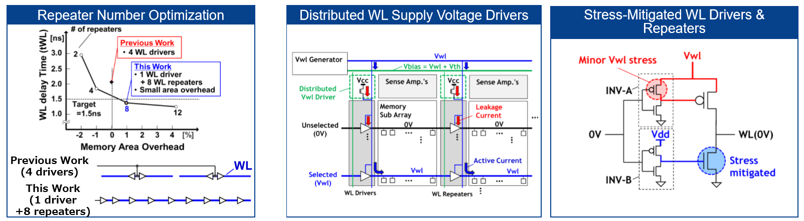
Word segmentation is an effective method to improve the random reading speed of embedded FLASH memory.However, this division increases the number of participle drivers and leads to reduced reliability due to the time-varying breakdown (TDDB) of the transistors contained in these drivers and the decrease in the voltage of the participle supply due to the increase in the leakage current.Renesas electronics solved these problems by using the word segment driver for pressure relief and distributed word segment power supply voltage driver, and validated the 240 MHz high speed random access at a wide temperature range (junction temperature from -40°C to 170°C), the highest in the industry in test chips.
Development of noise reduction technology
In programming flash memory, renesas reduced peak current consumption from external power sources (VCC) by 55% without reducing throughput compared to previous renesas devices by varying the write current applied to each storage cell between initial and subsequent operations.This inhibits the adverse effect of power voltage noise on the MCU itself during OTA operation while the vehicle is running.Renesas has also applied the idea of changing the write current to a high-speed write mode, in which the number of units programmed simultaneously increases.Thus, in this mode, the new device achieves high speed programming of 6.5MB/s.This makes it possible to suppress the increased test time associated with large memory capacity.

OTA can control both robust and high-speed software switching
In this test chip, the code storage flash memory is divided into storage areas for the software in use and storage areas for updating the software.This makes it possible to switch software in less than a millisecond (1/1000 second) when ignition is turned off.In addition, software switching Settings are repeated, and new status flags have been added to prevent incorrect operations from occurring if software updates or switches are inadvertently interrupted.This also allows robust operation, allows for reliable selection of executable control software, and reduces downtime when the vehicle is not in use.
These technologies make it possible to scale up automotive control software, high-speed real-time control, and advanced otas.Looking ahead, renesas is committed to the continued growth of embedded flash and to achieving the higher capacity, higher speed, and lower power consumption required to support new applications.
annotation
(note 1)MONOS: metal - oxide - nitride - oxide - silicon.Renesas electronics has a strong track record of using MONOS technology in EEPROM, security MCU and other products over the past 20 years.MONOS technology is used in the embedded FLASH memory of renesas MCU.
Renesas flash technology, announced at the 2015 international conference on solid-state circuits (ISSCC 2015).