In the FPGA high-speed AD acquisition design, PCB wiring errors will cause interference.Today small make up for you to introduce some wiring solutions.
1. Equal length of signal line
Take SDRAM or DDRII as an example, the data line, command line, address line and clock line should be the same length, the error should not exceed 500mil.

Above is the FPGA and SDRAM wiring, the clock frequency is set to 125M, in order to equal length can be serpentine line.
Although the serpentine routing can achieve the same line length, it also takes up more PCB area.Serpentine lines have no so-called filtering or anti-interference ability and can only reduce the signal quality, so they are only used for timing matching and have no other purpose.
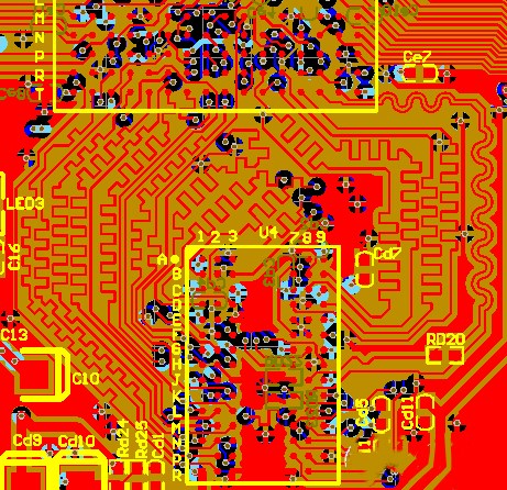
DDRII line of equal length design, the most right arc of the larger line for the difference of the clock line, the quality requirements of the clock line is relatively high.
Cabling is painful and cumbersome, and you'll need to rewire if you can't get it to work.
2. Power chip selection
In many cases of high speed AD, the switching power supply is not suitable because of the many burrs caused by the switching power supply.Most choose linear regulated power supplies.Taking ASM1117 as an example, I introduce the use of capacitors in power supply chips.
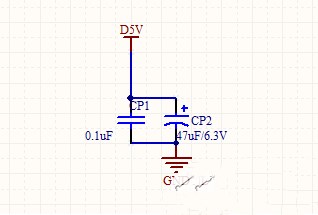
At the input end of 5V power supply, tantalum capacitors or electrolytic capacitors with large capacitance value should be added to filter out the low frequency noise of the power supply, and 104 (0.1uf) ceramic capacitors should be added to filter out the high frequency noise.The power line should be widened properly.
In PCB wiring, a capacitance with a large capacitance should be added at the end of 5V wiring.
Take asm1117-3.3 as an example, as shown in the figure below:

As shown in the figure above, if the 3.3 output of 1117 goes down, the capacitor CP5 will not have any effect if placed beside it. Usually, this kind of capacitor is 104 ceramic capacitors, and the capacitance of this capacitor is a very good one, which is very effective in power supply filtering.
So how do you lay it out?
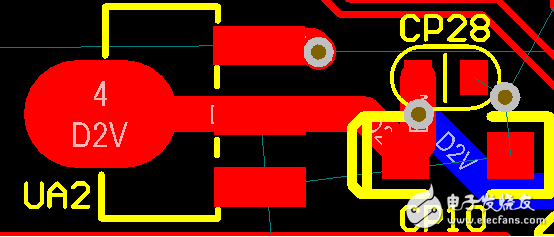
As shown in the figure above, for this layout, CP28 and CP10 are placed and the capacitors should be placed in the power supply routing path.Note that the capacitor should not be too far away from the chip pin. The capacitor has a filter radius, and if it goes beyond a certain range, the capacitor will not be able to filter.
FPGA power supply wiring, based on years of wiring experience and product stability, small make up for you to recommend the following scheme:

Take the FPGA encapsulated by QFP as an example, there are three power sources, 1.2v, 2.5v and 3.3v.When wiring, the best effect as above, the best distance between the power lines, FPGA power pin to add 104 capacitance.
3. Active crystal oscillator wiring
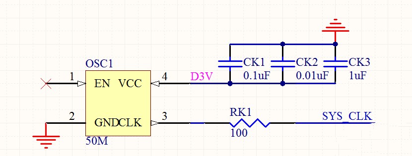
As shown in the schematic design, the clock output is connected with resistors of 100~330 ohms in series to prevent the reflection and superposition of the clock signal when the impedance is mismatched.
Three kinds of ceramic capacitor filters (103, 104 and 105) are added to the active crystal oscillator power supply to prevent the crosstalk between the power supply noise and the clock.
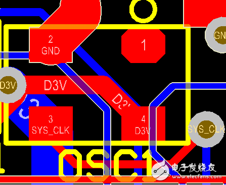
PCB wiring, the above effect is very bad.There should be no wiring under the crystal oscillator, and the power line should be away from the clock line, and the ground wire should be widened in the middle to prevent interference.
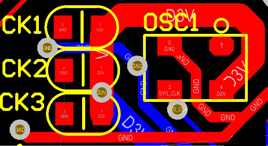
As the above wiring, the power line to avoid the clock line, the middle to join the thick ground wire, note that some ground wire does not need to be connected manually, place the hole, copper (ground network), will automatically join.

It is also possible to place capacitors in this manner.


 Inglês
  Chinês
  Alemão
  Coreano
  Japonês
  Farsi
Farsi  Portuguese
  Russian
  Espanhol
